
Introduction
In modern digital communication systems, high-speed data must travel through cables, printed circuit board traces, and backplanes while maintaining signal quality and reliability. As data rates increase, signals become more vulnerable to transmission losses, distortion, and timing errors. These problems can reduce the accuracy of data reception and make it difficult for electronic systems to operate reliably over longer distances.
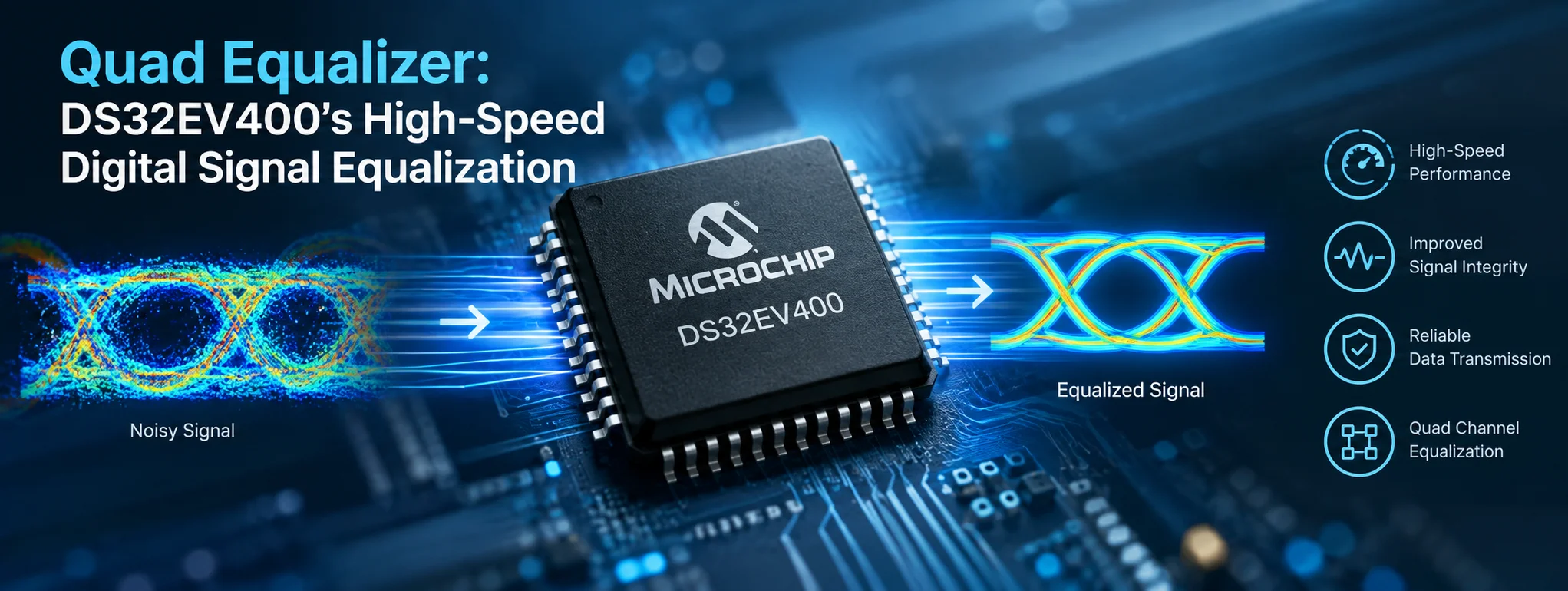
A quad equalizer is a device designed to compensate for signal degradation across multiple data channels. The Texas Instruments DS32EV400 is a programmable quad equalizer developed for high-speed digital data transmission. According to its datasheet, the device supports four non-return-to-zero (NRZ) data channels and is optimized for operation at data rates up to 3.2 gigabits per second (Gbps).
The DS32EV400 compensates for losses introduced by transmission media and helps reduce medium-induced deterministic jitter. It provides eight programmable levels of equalization, individual signal-detection outputs, channel-enable controls, and configuration through either external control pins or a Serial Management Bus (SMBus).
You can download :Quad Equalizer: DS32EV400’s High-Speed Digital Signal Equalization
These features make the device useful in applications such as DisplayPort, XAUI, InfiniBand, and other high-speed data transmission systems. Its purpose is to help maintain signal integrity when data travels through physical interconnects that would otherwise weaken or distort the transmitted signal.
1. Understanding the Quad Equalizer
The term quad refers to the four independent data channels integrated into the DS32EV400. Instead of requiring a separate equalizer for every signal path, the device provides four channels within a single component.
Each channel receives a high-speed differential signal, applies equalization to compensate for transmission losses, and passes the conditioned signal through additional internal circuitry before producing an output.
The four-channel design is useful in systems where multiple high-speed signals must travel between components. For example, a communication or computer system may need to transfer several data streams between an integrated circuit, a circuit board, and a cable or backplane.
As signals travel through these physical connections, their quality can deteriorate. The amount of degradation depends on factors such as the transmission medium, cable length, trace geometry, and signal frequency. Higher-frequency components of a digital signal are often attenuated more strongly than lower-frequency components, which changes the shape of the received waveform.
The DS32EV400 addresses this problem by providing configurable equalization strength. Engineers can select a suitable setting based on the expected loss of the transmission channel.
The datasheet identifies the device as a programmable quad equalizer optimized for backplane and cable applications at data rates up to 3.2 Gbps. It also describes support for both AC-coupled and DC-coupled data paths, allowing it to accommodate different interface designs.
2. Key Features and Specifications
The DS32EV400 combines signal-conditioning capabilities with configuration and power-management features. The principal specifications listed in the supplied datasheet include the following.
|
Feature |
Datasheet specification |
|---|---|
|
Number of data channels |
Four |
|
Maximum optimized data rate |
Up to 3.2 Gbps |
|
Programmable equalization |
Eight levels |
|
Equalization capability |
Up to 14 dB of loss at 3.2 Gbps |
|
Control methods |
External pins or SMBus |
|
Power supply |
2.5 V or 3.3 V |
|
Typical power consumption |
375 mW at 2.5 V |
|
Output type |
Differential current-mode logic (CML) |
|
Signal detection |
Independent detection for each channel |
|
Channel power control |
Independent enable and standby control |
|
Package |
7 mm × 7 mm, 48-pin leadless WQFN |
|
Operating temperature |
−40°C to +85°C |
|
Human-body-model ESD rating |
9 kV |
These specifications describe the device’s intended operating capabilities. Actual performance in a particular system depends on the channel, board design, configuration, and operating conditions.
The datasheet also reports residual deterministic jitter of 0.12 unit intervals (UI) at 3.2 Gbps with 40-inch FR4 traces under its stated conditions. This illustrates the device’s intended role in preserving signal quality over challenging transmission paths.
3. How Signal Equalization Works
Signal equalization is the process of compensating for distortions introduced when an electrical signal travels through a transmission medium.
A digital transmitter generates a sequence of electrical pulses representing binary data. Ideally, these pulses arrive at the receiver with clear transitions and sufficient amplitude for reliable interpretation. In a real transmission channel, however, the signal may experience attenuation, frequency-dependent loss, and waveform distortion.
For example, when a high-speed signal travels through a long PCB trace or cable, the higher-frequency components associated with sharp transitions can become weaker. The received waveform may consequently have slower edges and less clearly defined transitions. This can make it more difficult for the receiver to distinguish one bit from another, particularly at high data rates.
The DS32EV400 compensates for transmission-medium losses through its equalizer stage. By selecting an appropriate equalization setting, the device helps restore aspects of the signal that have been degraded by the channel.
The datasheet describes four principal functional blocks within each data channel:
-
Input termination: The incoming differential signal enters the channel through its differential input pins. The device includes an on-chip 100-ohm termination resistor between the input pair.
-
Equalizer: This stage compensates for signal degradation introduced by the transmission medium.
-
Limiting amplifier and DC offset correction: These internal blocks condition the signal following equalization.
-
CML output driver: The processed signal is delivered through a differential current-mode logic output pair.
Together, these blocks form the signal-conditioning path for each of the four channels.
Why equalization matters at high data rates
At high speeds, each bit occupies a shorter time interval. Consequently, signal distortion and timing uncertainty can have a greater effect on whether the receiver interprets the data correctly.
The DS32EV400 provides a way to compensate for the losses that arise in high-speed interconnects. Its programmable settings allow designers to adapt the equalization strength to the channel rather than using a single fixed level for every installation.
This flexibility is particularly relevant when a system must support different cable lengths or PCB routing distances.
4. Four Independent Data Channels
One of the DS32EV400’s defining characteristics is its integration of four equalizer channels in one device.
Each channel has its own differential input and output, equalizer circuitry, signal-detection output, and enable control. This arrangement allows the component to support systems carrying multiple high-speed data streams.
The four channels are identified as channels 0, 1, 2, and 3. Each has corresponding input pins, output pins, an enable input, and a signal-detect output.
The channel architecture offers two practical advantages.
First, it reduces the need to use a separate equalizer component for every data path. This can simplify the component arrangement on a circuit board when four compatible signal channels need conditioning.
Second, the independent enable and signal-detection functions allow each channel to be managed separately. A channel that is not currently receiving a usable signal does not necessarily need to remain fully active.
The datasheet’s application diagram illustrates the DS32EV400 in high-speed communication paths involving ASICs or FPGAs, switch-fabric cards, line cards, backplanes, and cables. These examples show how the device can sit between a transmitting or receiving subsystem and a transmission medium.
The appropriate system arrangement depends on the overall signal path and the electrical requirements of the connected equipment.
5. Eight Programmable Equalization Levels
The DS32EV400 supports eight equalization boost levels. These levels allow engineers to select compensation appropriate to the expected loss of the transmission channel.
The boost setting is selected using three control bits, designated BST_[2:0], when external-pin control is enabled. Three binary bits provide eight possible combinations, corresponding to the device’s eight equalization settings.
The datasheet provides the following illustrative relationship between boost settings and transmission media:
|
BST setting |
Example FR4 trace length |
Example 24-AWG Twin-AX cable length |
Listed channel loss at 1.6 GHz |
|---|---|---|---|
|
000 |
0 inches |
0 m |
0 dB |
|
001 |
5 inches |
2 m |
3 dB |
|
010 |
10 inches |
3 m |
6 dB |
|
011 |
15 inches |
4 m |
7 dB |
|
100 |
20 inches |
5 m |
8 dB |
|
101 |
25 inches |
6 m |
10 dB |
|
110 |
30 inches |
7 m |
12 dB |
|
111 |
40 inches |
10 m |
14 dB |
These values are the datasheet’s example channel-loss associations, not universal guarantees for every cable or PCB. Actual loss varies with the construction and electrical properties of the transmission medium.
The default boost setting is 100. The datasheet describes equalization of up to 14 dB of loss at 3.2 Gbps in its feature list.
Choosing the right equalization level
Selecting a boost level should be based on the expected transmission-channel loss and validated through measurements or system testing.
If the selected compensation is insufficient, the output may retain significant channel-induced distortion. Conversely, engineers should not assume that the highest boost setting will always produce the best result. The proper setting depends on the actual channel and the system’s signal-integrity requirements.
The availability of eight settings makes it possible to tune the device for different signal paths without changing the hardware component.
6. Configuration Through External Pins and SMBus
The DS32EV400 supports two main methods for configuring equalization: external control pins and the Serial Management Bus.
External-pin configuration
In pin-controlled operation, the BST_[2:0] pins determine the equalization boost setting. This approach is straightforward when a design requires a fixed setting or when the hardware uses shared configuration for all four channels.
The Force External Boost (FEB) pin determines whether the boost setting is controlled by the external pins or by SMBus registers. When FEB is held high, the external BST pins control the boost setting for all channels. FEB is internally pulled high, making pin-based boost control the default if the pin is left unconnected.
This method can be useful when a simple hardware configuration is preferred over software-controlled adjustment.
SMBus configuration
SMBus control provides more flexibility. When FEB is held low, equalization boost is controlled through the relevant SMBus registers. In this mode, each channel can be programmed individually.
The datasheet also documents register-based control for other functions, including channel enable behavior, signal-detection thresholds, and output amplitude.
The SMBus interface uses clock and bidirectional data signals, identified as SDC and SDA, along with a chip-select input. The CS pin enables access to the device’s SMBus registers when pulled high and disables register access when pulled low.
The documented bus operating-frequency range is 10 kHz to 100 kHz.
For a system designer, the choice between pin control and SMBus depends on whether the application needs a simple shared setting or independent, configurable channel behavior. In either case, the device should be configured according to the datasheet’s register definitions and electrical requirements.
7. Signal Detection and Channel Enable Control
Signal detection is an important feature of the DS32EV400 because it helps determine whether a usable input signal is present on a particular channel.
Each of the four channels has an independent signal-detect output, labelled SD0 through SD3. When the incoming differential signal exceeds the programmed signal-detection ON threshold, the corresponding output indicates that a signal has been detected.
When the signal falls below the OFF threshold, the output indicates that the signal is no longer sufficiently strong according to the selected detection setting.
The datasheet specifies the following default thresholds and alternative settings:
|
Threshold selection |
SD_OFF threshold |
SD_ON threshold |
|---|---|---|
|
00 — Default |
40 mV |
70 mV |
|
01 |
30 mV |
55 mV |
|
10 |
55 mV |
90 mV |
|
11 |
45 mV |
75 mV |
These values refer to differential input signal levels, as defined in the datasheet. The thresholds can be configured through SMBus registers.
The separate ON and OFF thresholds allow the device to distinguish between signal-present and signal-absent conditions without using a single identical switching threshold for both transitions.
Independent channel enable
Each channel also has an enable input. When the enable signal is high, the channel operates normally; when it is low, the channel enters standby mode.
This independent control is useful when a system does not always use all four channels. Unused channels can be placed in standby to reduce power consumption.
The device can also be configured to use its signal-detect output to control its enable input. With the required register configuration, connecting SDn to ENn allows a channel to become active when an input signal is detected and return to standby when the signal falls below the OFF threshold.
This automatic-enable feature can help reduce unnecessary power consumption in systems where the presence of incoming signals changes over time.
8. Power Consumption and Output-Level Control
Power efficiency is an important consideration in electronic systems containing multiple high-speed signal-conditioning components.
The DS32EV400 supports operation from either a 2.5 V or a 3.3 V power supply. The datasheet lists typical power consumption of 375 mW at 2.5 V.
Its standby mode helps reduce power consumption when a channel is not required. In standby, the control interface, including SMBus, and the signal-detection circuitry remain active, while the channel’s normal data-processing operation is disabled.
The datasheet also provides programmable output-amplitude settings through SMBus. The documented output levels are:
-
400 mV peak-to-peak
-
540 mV peak-to-peak
-
620 mV peak-to-peak, the default
-
760 mV peak-to-peak
These settings allow the output amplitude to be adjusted to suit the requirements of the connected system. Engineers should select a suitable output level after considering the receiver’s electrical specifications and the complete signal path.
9. Applications of the DS32EV400
The datasheet identifies several applications for the DS32EV400.
DisplayPort: The device can be used to extend the reach of DisplayPort high-speed video connections. The datasheet describes a typical example in which nominal cable reach can be increased from approximately six metres to twelve metres. The actual achievable distance depends on the cable and operating conditions.
XAUI: XAUI is a high-speed interface used in networking equipment. Equalization can help compensate for losses in the interconnects between compatible system components.
InfiniBand: High-speed interconnect systems require careful control of signal quality. The DS32EV400 is listed as a potential equalization component for this application area.
Other 8b/10b applications: The device supports balanced coding schemes such as 8b/10b. It also supports long-run-length data patterns such as PRBS-31, according to the datasheet.
These applications share a common requirement: high-speed data must travel through physical transmission channels without unacceptable signal degradation. The DS32EV400 addresses that requirement by offering configurable equalization across four channels.
10. PCB Layout and Hardware Design Considerations
Even a capable equalizer cannot compensate for every problem caused by poor circuit-board design. Proper layout and power distribution are therefore essential when implementing the DS32EV400.
The datasheet specifies an on-chip 100-ohm termination resistor between each differential input pair. It also documents output termination through on-chip 50-ohm resistors connected from the output pins to the supply.
Designers should follow the recommended differential-routing and interconnection practices appropriate to the interface. Maintaining suitable impedance, minimizing unnecessary discontinuities, and controlling the quality of the transmission path help preserve signal integrity.
The power-supply connections also require attention. The datasheet recommends connecting the VDD pins to the supply plane through a low-inductance path and placing a 0.01 µF bypass capacitor between each VDD pin and the ground plane. Ground connections should use a solid ground plane and a low-impedance path. The exposed package pad must also be connected to the board’s ground plane.
The DS32EV400 is supplied in a 7 mm × 7 mm, 48-pin leadless WQFN package. Designers must account for the package footprint, grounding, thermal considerations, and assembly requirements when creating the PCB.
The datasheet specifies an operating temperature range of −40°C to +85°C. Systems must remain within the device’s recommended operating conditions to achieve the intended performance.
11. Advantages and Design Limitations
The DS32EV400 offers several practical advantages. Its four-channel architecture consolidates equalization functions into one component, while its eight boost settings allow adjustment for different transmission losses. Independent signal detection and channel enable controls provide additional flexibility, and SMBus configuration supports per-channel tuning.
The device also supports both AC- and DC-coupled signal paths, making it suitable for a range of interface implementations.
However, designers must recognize that the component is not a universal solution to every signal-integrity problem. Its performance depends on the transmission channel, selected equalization, power supply, layout, and connected equipment. The datasheet’s example cable lengths and loss values should not be treated as guarantees for all installations.
Careful evaluation, correct configuration, and validation under the intended operating conditions remain necessary.
Conclusion
The Texas Instruments DS32EV400 is a programmable quad equalizer designed to improve signal integrity in high-speed digital communication systems. It provides four differential data channels, eight equalization boost levels, SMBus and external-pin configuration, independent signal detection, and per-channel standby control.
Its support for data rates up to 3.2 Gbps and its ability to compensate for transmission-medium losses make it relevant to applications involving DisplayPort, XAUI, InfiniBand, backplanes, and cables.
1 thought on “Quad Equalizer: DS32EV400’s High-Speed Digital Signal Equalization”